The complete guide to PCB pad :types, size, spacing, repair and
4.6 (373) In stock

Soldering is one of the most important processes in PCBA processing. On printed circuit boards, electrical connections to all components are made via PCB pads. The PCB pads are a very critical part of the PCB that determines where components are soldered on the PCB.The size, shape, and position of pads in a PCB directly depend on the manufacturing quality of the board. Today we will take a look at the PCB pad in SMT soldering.
Soldering is one of the most important processes in PCBA processing. On printed circuit boards, electrical connections to all components are made via PCB pad.
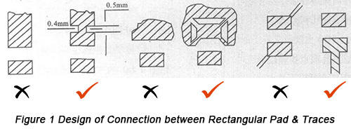
Design Requirement of SMT PCBs Part Two: Settings of Pad-Trace Connection, Thru-Holes, Test Point, Solder Mask and Silkscreen

Drilled Holes - Eurocircuits Eurocircuits

Getting to know PCB terminal blocks : function, material and sizes - IBE Electronics

PCB connector : definition, types, and how to choose and identify - IBE Electronics
PCB Pad Size Guidelines: Finding the Proper Pad Sizes for Your Circuit Design

What is a PCB pad - different types and design guidelines - PCBA Manufacturers

Getting to know PCB terminal blocks : function, material and sizes - IBE Electronics

Getting to know PCB terminal blocks : function, material and sizes - IBE Electronics

Getting to know PCB terminal blocks : function, material and sizes - IBE Electronics

How to maintain and clean PCB stencils for consistent performance? - IBE Electronics
The complete guide to PCB pad :types, size, spacing, repair and comparison - IBE Electronics
Flexible Wholesale Jacket Padding Materials For Clothing And More
html - Correct padding or margin when using fixed top bar - Stack
 RR Power Mesh Waist Cincher Brief 7049BK
 French sportswear retailer, Decathlon, cancels sale of hijab for women runners in France - The 51%
 38DD Balcony Bras, Balconette Push Up Bras
 Why Teaching Children to Identify Emotions is Important - ThinkPsych
 Women Full Body Shaper Seamless Tummy Control Underbust Waist Trainer Corset US
 Buy Jolie 5500g Silicone Padded Buttocks Underwear Hips Enhancer Women Body Shaper Fake Butt Panty for Drag Queen Crossdresser Online at desertcartEGYPT